


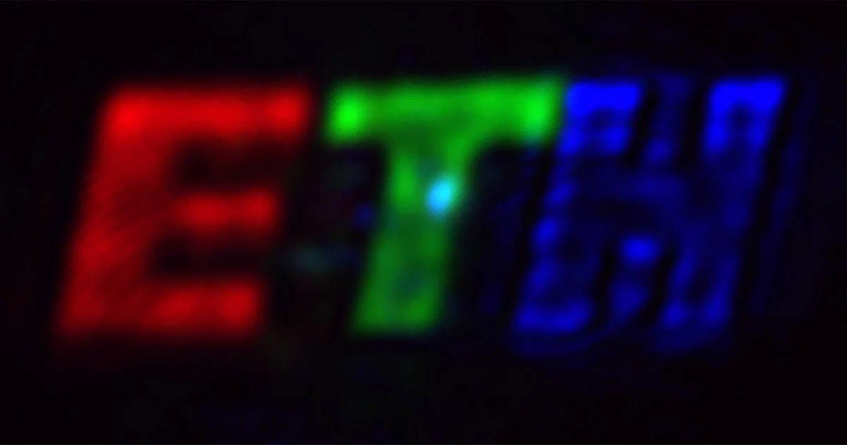
The landscape of digital imaging and display technology has remained fundamentally divided for nearly a century, separated by the functional distinction between sensors that record light and screens that emit it. This long-standing technological boundary has been challenged by a research team at ETH Zurich, led by David Norris, a Professor at the Optical Materials Engineering Laboratory. The team has successfully developed a "Fourier pixel," a groundbreaking optical component capable of both capturing and displaying images within a single unit. This innovation, detailed in a study published in the journal Nature in June 2026, marks a paradigm shift in optoelectronics, potentially paving the way for a new generation of hybrid devices where the distinction between a camera and a display ceases to exist.
The Evolution of the Pixel: From Wireless World to Bidirectional Control
To understand the magnitude of the ETH Zurich breakthrough, it is necessary to examine the historical trajectory of the pixel. The term "pixel," a portmanteau of "picture element," was popularized in the mid-20th century, though its conceptual roots trace back to early television experiments in the 1920s. For approximately 100 years, pixels have served as the fundamental building blocks of digital visual media, yet they have always operated as one-way streets. In a digital camera, a pixel—typically a photodiode—functions as a sensor, converting incoming photons into electrical signals to record an image. Conversely, in a display such as an OLED or LCD screen, a pixel functions as a light source or a shutter, converting electrical signals back into visible light.
Until now, these two functions required entirely different physical architectures. Integrating them into a single footprint has been a significant engineering hurdle, often resulting in "under-display" cameras that suffer from poor image quality due to the light-blocking properties of the screen layers above them. The Fourier pixel bypasses these structural limitations by utilizing the principles of wave optics and light interference, allowing a single surface to manipulate light in both directions simultaneously.
The Physics of Fourier Pixels: Interference and Surface Waves
The core of the ETH Zurich innovation lies in the manipulation of light waves through "sculpted surfaces" at the nanoscale. Traditional pixels rely on the intensity of light—the number of photons hitting a sensor or being emitted by a diode. The Fourier pixel, however, leverages the more complex properties of light: its oscillation phase and polarization.
When light strikes a surface, it scatters. The waves originating from various points on that surface overlap and interfere with one another. This interference can be constructive, where waves reinforce each other to create bright spots, or destructive, where waves cancel each other out to create dark spots. By precisely engineering the topography of the pixel’s surface, the researchers can control how these waves propagate.
The process involves converting incoming light into "surface waves" that travel across the chip’s surface. At specific intervals or positions within the pixel, these surface waves are scattered back out as light waves. By calculating the exact surface patterns required using Fourier analysis—a mathematical method used to decompose signals into their constituent frequencies—the researchers can dictate the resulting image or light pattern. This allows the pixel to "steer" light for display purposes while simultaneously "analyzing" incoming light for imaging purposes.
Technical Capabilities and Experimental Results
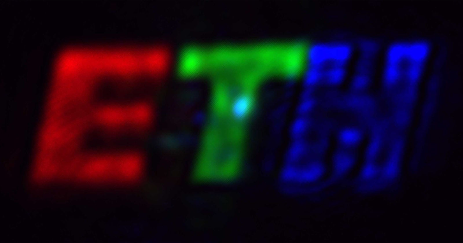
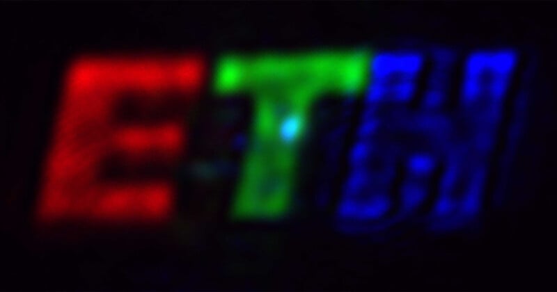
The research paper, titled "Fourier pixels for bidirectional light control," demonstrates that these pixels are not limited to simple light detection. They can analyze the intensity, phase, and polarization of incoming waves. In the experimental phase, the team successfully created a colored logo using the Fourier pixels. The letter "E" in the logo was approximately 1 millimeter tall, demonstrating the high level of precision achievable at the microscopic level.
One of the most significant aspects of this technology is its ability to process information optically. According to Professor Norris, these pixels can react to a captured image and produce a corresponding light response without the intervention of a traditional computer processor. This "analog" optical processing could significantly reduce latency and power consumption in complex imaging systems.
The team has already moved toward practical implementation by developing a matrix of Fourier pixels. Unlike a single pixel, a matrix allows for the creation of complex, high-resolution images and the simultaneous capture of multi-dimensional visual data. This scalability is crucial for the transition from a laboratory concept to a commercially viable technology.
Chronology of Development and Recognition
The development of the Fourier pixel is the result of years of research at the Optical Materials Engineering Laboratory at ETH Zurich. The timeline of the project reflects a rigorous path from theoretical physics to experimental validation:
- Early 2020s: Initial research into surface plasmons and nanophotonics begins at ETH Zurich, focusing on how light interacts with engineered metal and semiconductor surfaces.
- 2024-2025: The team refines the Fourier analysis models required to "program" the surface topography of the pixels. Experimental prototypes are developed to test bidirectional light control.
- June 24, 2026: The research is officially published in Nature, providing the global scientific community with the first comprehensive look at the Fourier pixel’s architecture and performance.
- Late 2026: The technology is nominated for the ETH Zurich Spark Award, which recognizes the most promising inventions from the university that lead to patent applications and have high commercial potential.
The filing of a patent application indicates that ETH Zurich views the Fourier pixel as a foundational technology for the future of the electronics industry.
Potential Impact on Consumer Electronics and Industry
The implications of bidirectional pixels are vast, particularly for the consumer electronics sector. Currently, manufacturers of smartphones and laptops struggle with the "notch" or "hole-punch" designs required to house front-facing cameras. Under-display camera technology has seen limited success due to the interference caused by the display pixels sitting on top of the sensor. A Fourier pixel array would eliminate this conflict entirely, as the screen itself would be the camera.
Beyond smartphones, the technology has transformative potential for Augmented Reality (AR) and Virtual Reality (VR). In AR glasses, Fourier pixels could allow for a more compact design where the lenses both track the user’s eye movements (capture) and project digital overlays (display) using the same optical elements. This would reduce the bulk of current headsets and improve the alignment between digital and physical worlds.
In the field of autonomous vehicles, Fourier pixels could lead to more integrated sensor suites. A vehicle’s headlights, for instance, could be replaced with Fourier pixel arrays that not only illuminate the road but also act as high-resolution LIDAR sensors, capturing three-dimensional data about the environment through the same aperture used for lighting.
Expert Reactions and Future Challenges
While the academic community has hailed the research as a "breakthrough," industry analysts suggest that several hurdles remain before Fourier pixels appear in consumer devices. Dr. Simon Vonk, one of the co-authors of the study, noted that the current challenge lies in the mass production of these complex nanostructures. The precision required to sculpt the pixel surfaces is currently achieved using advanced lithography, which can be expensive and time-consuming at scale.
Furthermore, integrating Fourier pixels with existing CMOS (Complementary Metal-Oxide-Semiconductor) manufacturing processes—the standard for modern electronics—will require significant cross-industry collaboration. However, the potential for "computer-less" optical processing has caught the attention of AI hardware developers, who see the Fourier pixel as a way to perform edge-computing tasks at the speed of light.
Conclusion: A New Era of Optical Integration
The work of David Norris and his team at ETH Zurich represents more than just a new type of hardware; it represents a fundamental shift in how humans interact with light and digital information. By collapsing the distance between the capture and the display of light, the Fourier pixel removes a century-old barrier in engineering.
As the technology matures, it is likely to redefine the aesthetics and functionality of digital devices. The transition from unidirectional pixels to bidirectional Fourier pixels could eventually lead to "smart surfaces" where any part of an object—a window, a car body, or a wall—can serve as both an eye and a voice, seeing and showing the world in a single, seamless interaction. For now, the successful patent application and the publication in Nature serve as the opening chapters of what may be the next great revolution in optoelectronics.

